Product Summary
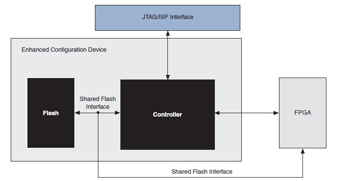
The EP2C50F672I8 is an Enhanced Configuration Device which contains a two-dimensional row- and column-based architecture to implement custom logic. Column and row interconnects of varying speeds provide signal interconnects between logic array blocks (LABs). The EP2C50F672I8 is embedded memory blocks, and embedded multipliers.
Parametrics
EP2C50F672I8 absolute maximum ratings: (1)Supply voltage: -0.2 to 4.6V; (2)Input voltage: -0.5 to 3.6V; (3)DC output current: -25 to 25mA; (4)Power dissipation: 360mW; (5)DC output current, per pin: -25 to 25 mA; (6)Storage temperature: -65 to +150℃; (7)Junction temperature: 135℃.
Features
EP2C50F672I8 features: (1)Standard flash die and a controller die combined into single stacked chip package; (2)Flash memory block/sector protection capability via external flash interface; (3)Pin-selectable 2-ms or 100-ms power-on reset (POR) time; (4)External clock source with frequencies up to 100 MHz; (5)Supply voltage of 3.3 V (core and I/O); (6)Standby mode with reduced power consumption.
Diagrams

| Image | Part No | Mfg | Description |  |
Pricing (USD) |
Quantity | ||||||
|---|---|---|---|---|---|---|---|---|---|---|---|---|
 |
 EP2C50F672I8 |
 |
 IC CYCLONE II FPGA 50K 672-FBGA |
 Data Sheet |

|
|
||||||
 EP2C50F672I8N |
 |
 IC CYCLONE II FPGA 50K 672-FBGA |
 Data Sheet |

|
|
|||||||
 (China (Mainland))


